The latest silicon chips unlock new capabilities, and this feature invites you to peek behind the curtain. From a sketch on a whiteboard to a finished wafer, the journey blends engineering rigor with global collaboration. Understanding silicon chip design choices helps readers appreciate how performance, power, and reliability are balanced. The evolution of lithography pushes patterning toward finer scales, including advances like EUV lithography. These moves are not just about speed; they affect energy efficiency, thermals, and reliability across devices.
In today’s discourse, these advances unfold as cutting-edge microprocessors and state-of-the-art integrated circuits, powered by careful design and manufacturing choices. Across the supply chain, terms like semiconductor manufacturing, wafer fabrication, and advanced lithography describe the same journey from concept to thousands of silicon devices. As researchers push toward the 3nm process node, materials science, thermal engineering, and packaging sophistication become as important as transistor density. This lens emphasizes chip fabrication technology and the ecosystem of tools, masks, and cleanrooms that translate designs into reliable, energy-efficient products. By using related terms and concepts, readers get a richer view of how tiny changes in process flow ripple through performance and cost.
Design and Architecture: Foundations of the Latest Silicon Chips
Design begins with a problem to solve and a clear target market. In silicon chip design, engineers balance cores, memory hierarchy, and accelerators to meet performance, power, and cost constraints. They rely on electronic design automation (EDA) tools that simulate timing, verify correctness, and help predict real-world behavior before any silicon is manufactured. The latest silicon chips are defined not by raw speed alone, but by energy efficiency, thermal profiles, and sustained performance under varied workloads.
This phase also hinges on close software collaboration. Compilers, runtimes, and system software must be able to leverage the hardware effectively, which means design teams work with software developers to align interfaces and microarchitectures with compiler optimizations. The outcome is a holistic system that reflects both innovative silicon chip design and the realities of semiconductor manufacturing that turn a whiteboard idea into mass-produced devices.
Verification, IP Integration, and Tape-Out in Modern Chip Fabrication Technology
Verification, IP integration, and manufacturing readiness form the gatekeepers between concept and production. Engineers assemble dozens of IP blocks, run exhaustive test suites, and simulate worst‑case power and timing scenarios to prevent bugs from reaching silicon. Layout versus schematic (LVS) checks and design rule checks (DRC) are standard steps to ensure manufacturability, and tape-out marks the moment the design is handed to the fabrication ecosystem.
Making a chip at scale requires a robust semiconductor manufacturing network: foundries, mask shops, wafer suppliers, and testers all coordinate with the design team. This collaboration reduces risk, protects yield, and keeps product cycles on schedule, underscoring that modern chip fabrication technology is as much about ecosystem design as it is about transistor physics.
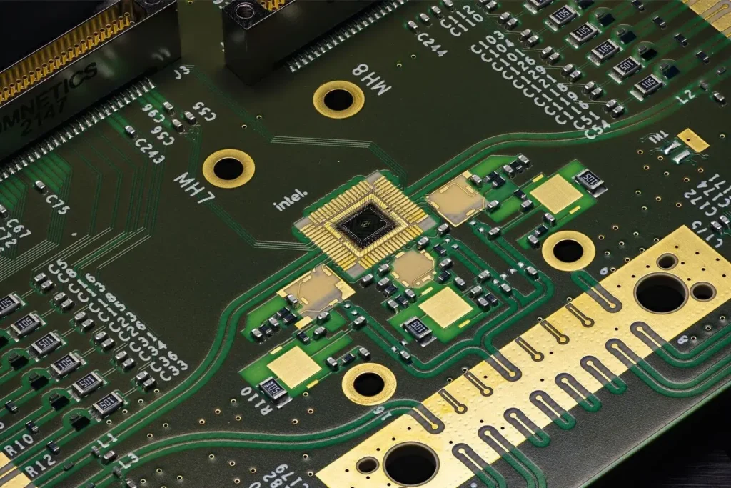
From Wafers to Devices: The Fabrication Journey and EUV Lithography
Fabrication begins with the wafer as a circular silicon canvas. High‑purity silicon ingots are grown by methods such as the Czochralski process, then sliced, lapped, and polished before the long sequence of deposition, diffusion, and etching that creates transistors and interconnects. Each layer adds features that will become memory arrays and logic blocks, and controlling impurities, stress, and surface topology is critical for uniform yield and predictable performance in the final devices. The move toward advanced lithography and precision CMP sits at the heart of chip fabrication technology.
Photolithography, and specifically EUV lithography, enables tighter patterning with fewer mask steps, pushing toward nanometer-scale features. EUV systems demand pristine optics and controlled environments, yet integration with deposition, etching, and CMP processes remains essential for consistent device behavior across billions of transistors. The result is a manufacturing sequence that translates raw silicon into dense, high‑performance circuits found in phones, data centers, and AI accelerators.
3nm Process Node Advancements: Transistors, Materials, and Thermal Management
Transistor technology is the engine of performance gains. The industry has moved from FinFETs toward gate‑all‑around (GAA) architectures, reshaping materials and device physics to achieve faster switching and lower power. In the 3nm process node, density increases and new materials and strain engineering enable higher performance within tight thermal budgets, while still facing the realities of interconnect scaling and packaging dependencies in silicon chip design and fabrication.
Realizing reliable operation at 3nm requires refined process control, novel materials, and advanced thermal management. The 3nm node illustrates the ongoing interplay between transistor density, interconnect performance, and packaging integration, highlighting that silicon chip engineering is as much about thermal budgets and leakage control as it is about gate length. The outcome influences chip fabrication technology across the supply chain and shapes product options for mobile, compute, and AI workloads.
Testing, Yield, and Production Readiness: Reliability at Scale
Even after wafers emerge from the fab, testing and yield determine feasibility at scale. Electrical and physical tests identify defects, while reliability assessments guard long‑term performance. Yield, the share of functional devices per wafer, drives cost and schedule, so manufacturing teams optimize process windows, inspection steps, and repair strategies within semiconductor manufacturing workflows.
Packaging closes the loop, optimizing thermal performance and electrical connectivity for real-world workloads—from gaming to cloud inference. At scale, tests across varied temperatures and voltages validate robustness, while packaging approaches in modern chips help meet energy efficiency and form factor goals. In short, testing, yield, and production readiness are the final gatekeepers that translate design intent into dependable products that customers can trust.
Economics, Supply Chains, and Global Collaboration Behind Silicon Innovation
Economics and supply chains shape what is feasible in silicon innovation. Fab capacity and capital expenditure run into the tens of billions for modern fabrication facilities, and the global network of chemical suppliers, gas suppliers, and equipment makers underpins semiconductor manufacturing. Regional diversification helps hedge risk, while multi‑site manufacturing allows throughput and resilience in the face of disruptions.
Geopolitics, policy, and standardization influence how quickly the latest silicon chips reach market. Collaboration among designers, foundries, and researchers—paired with a stable, transparent supply chain—enables consistent performance across devices and regions. The result is a global choreography where silicon chip design, semiconductor manufacturing, and advanced lithography coordinate to deliver next‑generation technology to consumers and enterprises alike.
Frequently Asked Questions
How does silicon chip design influence the performance, power efficiency, and AI capabilities of the latest silicon chips?
In the latest silicon chips, silicon chip design decisions—such as core counts, memory hierarchy, and integrated accelerators—drive performance and energy efficiency. Engineers rely on advanced EDA tools to simulate timing, verify correctness, and optimize for real workloads. Close collaboration with software stacks ensures compilers and runtimes exploit hardware features, balancing performance, power and area.
Why is EUV lithography critical for the latest silicon chips, and what benefits does it bring to pattern density?
EUV lithography enables finer patterning, higher density, and fewer mask steps, which are essential for making smaller transistors in the latest silicon chips. It requires pristine optics, controlled environments, and seamless integration with deposition and CMP steps to maintain yield and reliability.
What does the 3nm process node mean for the latest silicon chips in terms of density, performance, and power?
The 3nm process node represents higher transistor density and faster switching, enabled by gate-all-around designs and new materials. It improves performance per watt but demands stricter thermal budgets, improved strain engineering, and tighter integration with packaging to realize gains in mobile, PC, and data-center chips.
How does semiconductor manufacturing evolve from wafers to packaging for the latest silicon chips?
Semiconductor manufacturing covers wafer production, deposition, diffusion, etching, and CMP, advancing toward higher yields and tighter controls. The journey ends with advanced packaging that optimizes thermal performance, electrical interconnects, and mechanical robustness, ensuring the latest silicon chips reach devices reliably.
How do verification, LVS/DRC checks, and tape-out impact the manufacturing readiness of the latest silicon chips within chip fabrication technology?
A robust verification regime, LVS/DRC checks, and a smooth tape-out are essential for manufacturing readiness. These steps reduce functional bugs, ensure manufacturability, and synchronize design with fabrication capability across global foundries and mask shops.
What supply chain and global collaboration factors shape the delivery of the latest silicon chips in semiconductor manufacturing contexts?
Delivery depends on a coordinated semiconductor manufacturing ecosystem—foundries, mask shops, wafer suppliers, and chemicals—plus geopolitical and logistics considerations. Strong supplier diversification and standardization help manage risk and keep cycles aligned from design to volume production.
| Aspect | Key Points |
|---|---|
| Design and Architecture | Define target performance, power, area, and cost; set high-level architecture (cores, memory hierarchy, accelerators); use EDA tools to simulate behavior, verify timing, and ensure functional correctness; emphasize energy efficiency, thermal behavior, and real-workload performance; collaborate with software teams to ensure compilers and runtimes leverage hardware. |
| Verification, Compliance, and Tape-Out | Rely on dozens of IP blocks and exhaustive test suites; simulate worst-case power and timing scenarios; apply LVS and DRC checks to ensure manufacturability; aim for tape-out with minimal late-stage changes; maintain a robust supply chain of foundries, mask shops, wafer suppliers, and testing facilities; ensure design–fabrication collaboration to manage risk. |
| Fabrication | Wafer is the silicon canvas; ingot grown by methods such as Czochralski; deposition, diffusion, and etching create transistors, interconnects, and memory arrays; control of impurities, stress, and surface topology is critical; thermal management and contamination control in cleanrooms ensure millions of devices per wafer behave consistently. |
| Photolithography and EUV | EUV enables tighter patterning and higher density; traditional DUV evolved, but EUV requires pristine environments and ultra-pure optics; must harmonize lithography with etching, deposition, and CMP to maintain viability across billions of devices; EUV drives nanometer-scale features in latest silicon chips. |
| Transistors, Nodes, and the 3nm Frontier | Transistor technology centers on FinFETs and the shift to gate-all-around (GAA) structures; new materials and architectures aim for faster switching and better energy efficiency; 3nm represents a milestone with material, strain engineering, and thermal budget requirements; node labels are marketing shorthand, while actual challenges include transistor density, interconnect scaling, and packaging interplay. |
| Testing, Yield, and Production Readiness | Post-fabrication electrical testing, physical inspections, and reliability assessments identify defects; yield drives economics and scheduling; packaging optimization is essential for thermal performance and electrical/mechanical robustness; chips must survive real-world workloads across varied temperatures and voltages, with alignment from lithography to packaging. |
| Economics, Supply Chains, and Global Collaboration | Fab capacity is expensive; capital expenditure runs into tens of billions for modern facilities; a global ecosystem spans multiple regions with chemicals, gases, photoresists, and equipment; geopolitics and logistics shape rollout speed; designs can be produced at multiple sites to hedge risk, requiring standardization across tooling for uniform behavior. |
| Impact on Devices and Industry Trends | Consumers gain smarter devices, longer battery life, and higher performance ceilings; enterprises see faster AI workloads and lower total cost of ownership through efficiency gains; trends like chiplets, heterogeneous integration, and advanced packaging broaden ways to combine silicon functionality with real-world systems; breakthroughs ripple through product lines and ecosystems. |
Summary
Latest silicon chips continue to redefine what is possible across mobile, desktop, and data-center systems, delivering smarter performance, longer battery life, and new capabilities. The journey from a creative idea on a whiteboard to a silicon wafer—through design, verification, fabrication, lithography, and packaging—remains a coordinated global effort driven by thousands of decisions and a web of partnerships. As researchers push toward smaller nodes, advanced materials, and innovative architectures like gate-all-around transistors and chiplets, the ongoing evolution promises more powerful, efficient, and reliable chips that shape the devices and industries we rely on every day.